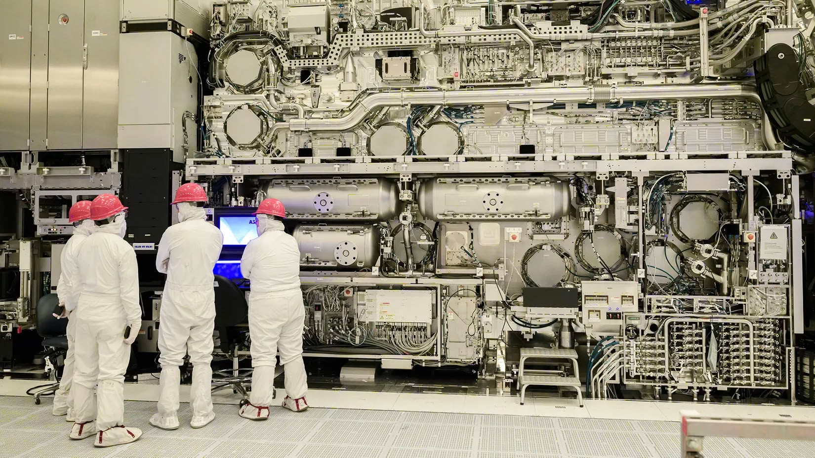
Intel has officially processed one million 300 mm silicon wafers using High Numerical Aperture (High NA) Extreme Ultraviolet (EUV) lithography, as confirmed by the company yesterday. Using High-NA in silicon manufacturing presents many challenges due to the additional complexity it introduces, but for Intel, the opposite is true.
Initially, Intel installed ASML's TWINSCAN EXE:5000 High-NA EUV systems in 2024 for research and testing of the 14A node. However, since then, Intel has found more useful ways to employ High-NA tools beyond the 14A node, extending their use to the 18A node, which was previously believed to be exclusive to 14A.
For a select subset of "Panther Lake" SKUs, Intel is etching a few layers of silicon using High-NA exposure, instead of solely relying on Low-NA. Furthermore, Intel is offering this High-NA setup to external customers, as it could be beneficial for them as well.
In collaboration with ASML, Intel has completed acceptance testing at Intel Foundry for its 14A node to enhance wafer output. This is done using TWINSCAN EXE:5200B, which is ASML's second version of High-NA EUV scanners, following the TWINSCAN EXE:5000 that Intel initially used for its 14A trial runs.
Intel previously reported processing over 30,000 wafers in a single quarter, achieving simplified manufacturing by reducing the steps needed for a specific layer from 40 to fewer than 10, resulting in significantly faster cycle times. Read full story